
Yield acceleration at the core
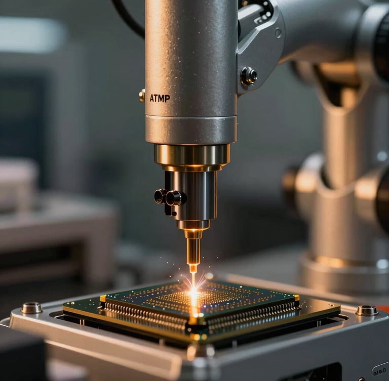
We modernize the silicon engineering lifecycle. By compiling deep-tech AI, spatial overlays, and sovereign data architectures directly into fabrication workflows, we drive sub-micron precision from design to ATMP.
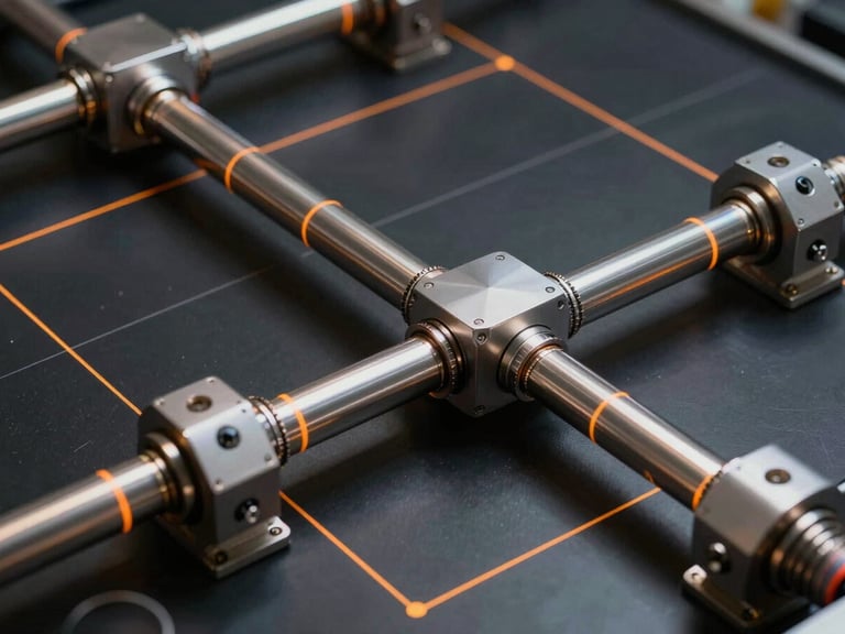
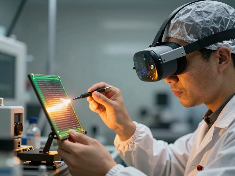
AXIS FRAMEWORK IN ACTION
Three vectors of silicon optimization
We deploy targeted deep-tech solutions across critical bottlenecks in the semiconductor lifecycle, replacing legacy friction with sovereign-grade intelligence.
Data Engineering Modernization
We migrate highly sensitive legacy fab logs and unstructured telemetry into high-throughput, sovereign data pipelines. This ensures real-time analysis of sub-micron anomalies without compromising intellectual property.
Assistive Systems & Automation
By deploying spatial overlays and eXtended Reality interfaces directly onto the fabrication floor, we reduce cleanroom turnaround times and accelerate manual verification cycles.
AI Systems Modernization
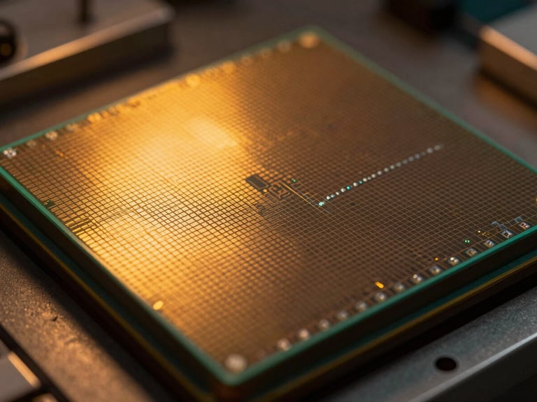
We compile custom deep-learning models optimized specifically for RTL-to-GDSII verification, automating optical inspections and identifying defect patterns before fabrication begins.
Quantifiable yield acceleration
Our deep-tech engineering engagements deliver verified operational gains across global and domestic semiconductor environments, optimizing throughput and micro-component precision.
99.8%
-40%
10x
Achieved in automated optical inspections of sub-micron wafer defects, eliminating manual inspection bottlenecks.
Realized in cleanroom turnaround times through high-precision spatial overlay assistance and interactive XR automation.
Accelerated telemetry processing achieved via modernized, air-gapped sovereign data pipelines deployed on-site.
SECURE ENGAGEMENT
Initiate technical evaluation
Partner with Akshavriddhi to integrate AXIS intelligence directly into your silicon design, fabrication, or ATMP pipeline. Our secure portal is open for sovereign and enterprise consultations.